
Nanotechnology
Review of plasma etching processes for III-V semiconductors
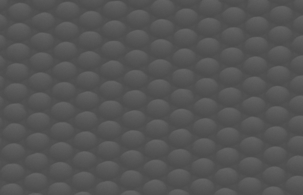
Front Surface Nanotexturing for Increased Optical Generation Rate in GaAs Photovoltaic Devices
III-V Nanotexturing for Improved Light Trapping and Reduced Costs
3D interconnects for III-V semiconductor heterostructures for miniaturized power devices
III-V/Ge Multijunction Solar Cell with Through Cell Via Contact Fabrication and Characterization
Influence of plasma process on III-V/Ge multijunction solar cell via etching